Beschreibung
Der Baustein CD4066B ist ein vierseitiger bilateraler Schalter, der für die Übertragung oder das Multiplexing von analogen oder digitalen Signalen vorgesehen ist. Er ist Pin-für-Pin-kompatibel mit dem CD4016B-Baustein, weist aber einen wesentlich geringeren Durchlasswiderstand auf. Darüber hinaus ist der Durchlasswiderstand über den gesamten Signaleingangsbereich relativ konstant. Der CD4066B-Baustein besteht aus vier bilateralen Schaltern, die jeweils unabhängig voneinander gesteuert werden. Sowohl das p- als auch das n-Bauelement in einem bestimmten Schalter werden durch das Steuersignal gleichzeitig ein- oder ausgeschaltet. Wie in Abbildung 17 dargestellt, ist die Quelle des n-Kanal-Bauelements an jedem Schalter entweder mit dem Eingang (wenn der Schalter eingeschaltet ist) oder mit VSS (wenn der Schalter ausgeschaltet ist) verbunden. Diese Konfiguration eliminiert die Variation der Schwellenspannung des Schaltertransistors mit dem Eingangssignal und, hält somit den Einschaltwiderstand über den gesamten Betriebssignalbereich niedrig. Die Vorteile gegenüber einkanaligen Schaltern sind Eingangssignal-Spitzenspannungsschwankungen, die der vollen Versorgungsspannung und eine konstantere On-State Impedanz über den Eingangssignalbereich. Für Sample-and-Hold-Anwendungen wird jedoch der CD4016B-Baustein empfohlen.
Eigenschaften
- 15-V-Digital- oder ±7,5-V-Spitzenwert-Umschaltung
- 125-O typischer Durchgangswiderstand für 15-V-Betrieb
- Einschaltwiderstand des Schalters mit einer Genauigkeit von 5 O über den 15-V-Signaleingangsbereich
- Durchgangswiderstand flach über den gesamten Spitzenwert-Signalbereich
- hoch Ein- oder Ausschalt-Ausgangsspannungsverhältnis: 80 dB typisch bei fis = 10 kHz, RL = 1 kO
- hoher Grad an Linearität: <0,5% Verzerrung typisch bei fis = 1 kHz, Vis = 5-Vp-p
VDD - VSS = 10-V, RL = 10 kO
- extrem niedrige Schalterleckage im Aus-Zustand, was zu einem sehr niedrigen Offset-Strom und einem hohen effektiven Aus-Zustands-Widerstand führt: 10 pA typisch bei VDD - VSS = 10-V, TA = 25°C
- extrem hohe Steuereingangsimpedanz (Steuerkreis isoliert vom Signalkreis):
1012 O typisch
- geringes Übersprechen zwischen Schaltern: -50 dB typisch bei fis = 8 MHz, RL = 1 kO
- angepasste Steuereingangs- zu Signalausgangskapazität: Reduziert Ausgangssignal-Transienten
- Frequenzgang, Einschalten = 40 MHz typisch
- 100% Getestet auf Ruhestrom bei 20 V
- 5-V-, 10-V- und 15-V-Parameterwerte
Anwendungen
- Analoges Signal Switching und Multiplexing: Signaltorsteuerung, Modulatoren, Squelch-Steuerungen, Demodulatoren, Chopper, Kommutierungsschalter
- Digitales Signal Switching und Multiplexing
- Implementierung von Übertragungs-Gate-Logik
- Analog-zu-Digital- und Digital-zu-Analog-Wandlungen
- digitale Steuerung von Frequenz, Impedanz, Phase, und Analogsignal-Verstärkung
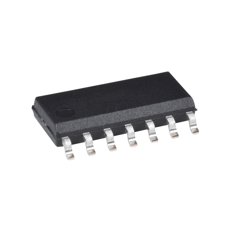
Auf Lager
SKU CD 4066BM TEX
Switch, Quad, 3 ... 18 V, SO-14
MPN CD4066BM
Hersteller TEXAS INSTRUMENTS
0,49 €
Technische Daten
Allgemeines
Familie
4000B
Modell
Analog Switch
Ausführung
bilateral
Bauform
DIP-14
Herstellerangaben
Hersteller
TEXAS INSTRUMENTS
Artikelnummer des Herstellers
CD4066BM
Verpackungsgewicht
1.0E-4 kg
RoHS
konform
EAN/GTIN
9900002165596
Statistische Warennummer
85423990
Sicherheitsinformationen
Verantwortliche Person für die EU
In der EU ansässiger Wirtschaftsbeteiligter, der sicherstellt, dass das Produkt den erforderlichen Vorschriften entspricht:
Texas Instruments Deutschland GmbH
Haggertystr. 1
85356 Freising, DE
[email protected]
https://www.ti.com
0,49 €
999 auf Lager
Versand heute bei Bestellung bis 16 Uhr
Versand heute bei Bestellung bis 16 Uhr
✓ Versand heute bei Bestellung bis 16 Uhr
✓ Rechnung mit ausgewiesener MwSt.
✓ 30 Tage Rückgaberecht